Intel Unveils Lunar Lake Architecture: New P and E cores, Xe2-LPG Graphics, New NPU 4 Brings More AI Performance
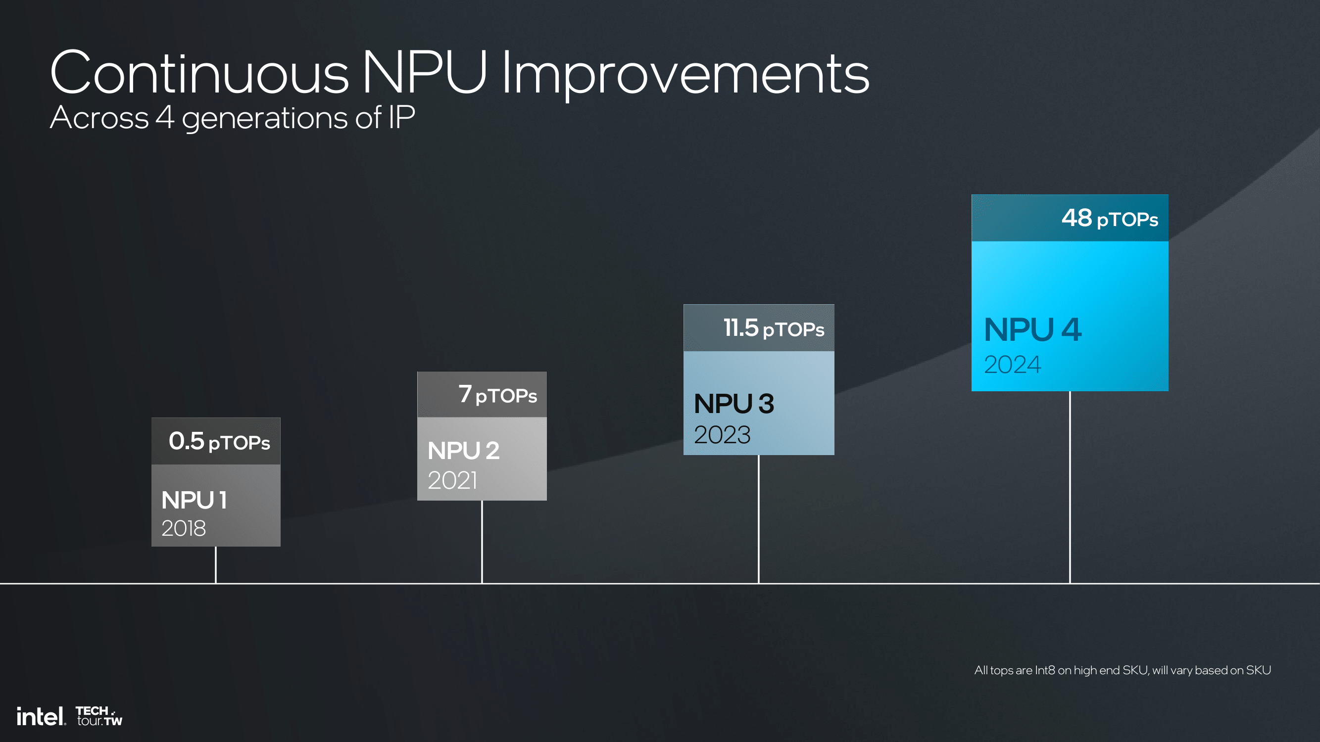
by Gavin Bonshor on June 3, 2024 11:00 PM ESTNew NPU: Intel NPU 4, Up to 48 Peak TOPS
Perhaps Intel's main focal point, from a marketing point of view, is the latest generational change to its Neural Processing Unit or NPU.Intel has made some significant breakthroughs with its latest NPU, aptly called NPU 4. Although AMD disclosed a faster NPU during their Computex keynote, Intel claims up to 48 TOPS of peak AI performance.NPU 4, compared with the previous model, NPU 3, is a giant leap in enhancing power and efficiency in neural processing. The improvements in NPU 4 have been made possible by achieving higher frequencies, better power architectures, and a higher number of engines, thus giving it better performance and efficiency.
In NPU 4, these improvements are enhanced in vector performance architecture, with higher numbers of compute tiles and better optimality in matrix computations.This incurs a great deal of neural processing bandwidth; in other words, it is critical for applications that demand ultra-high-speed data processing and real-time inference. The architecture supports INT8 and FP16 precisions, with a maximum of 2048 MAC (multiply-accumulate) operations per cycle for INT8 and 1024 MAC operations for FP16, clearly showing a significant increase in computational efficiency.
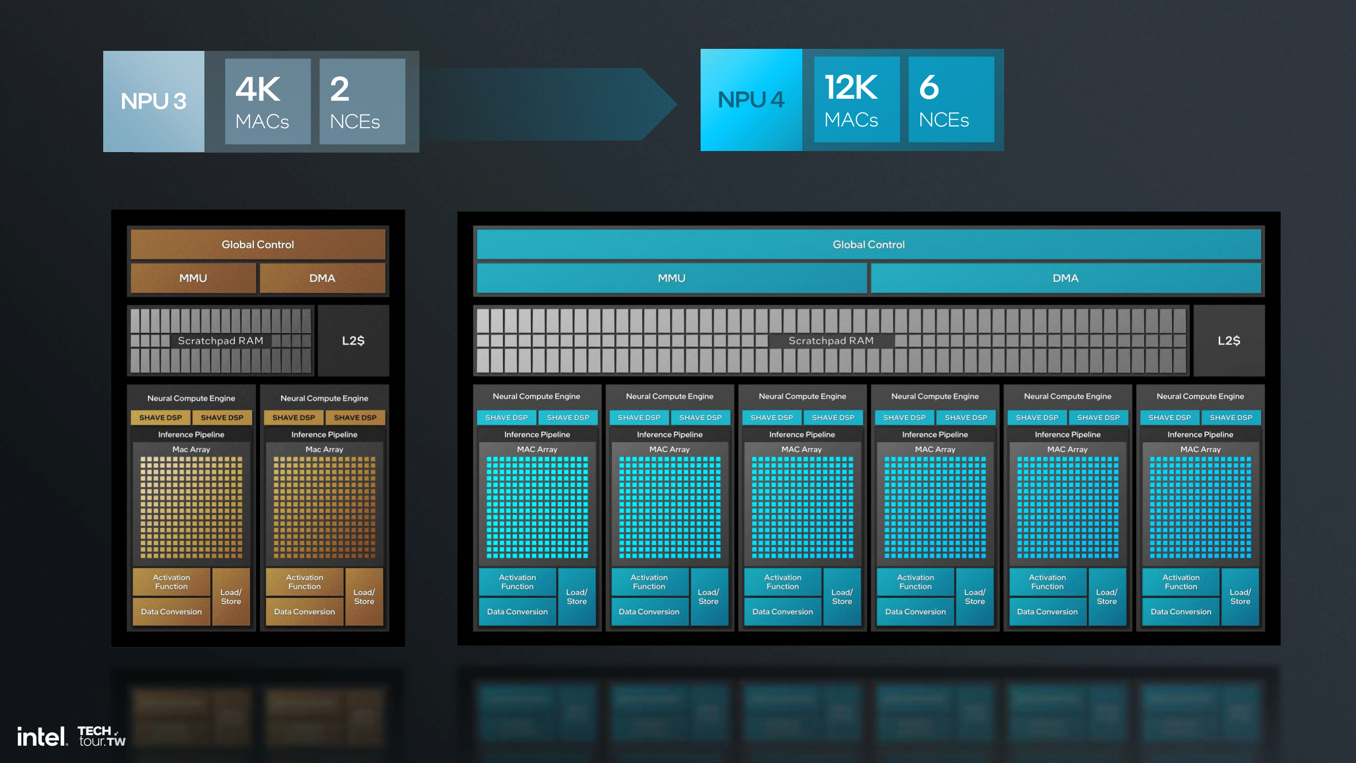
A more in-depth look at the architecture reveals increased layering in the NPU 4. Each of the neural compute engines in this 4th version has an incredibly excellent inference pipeline embedded — comprising MAC arrays and many dedicated DSPs for different types of computing. The pipeline is built for numerous parallel operations, thus enhancing performance and efficiency. The new SHAVE DSP is optimized to four times the vector compute power it had in the previous generation, enabling more complex neural networks to be processed.
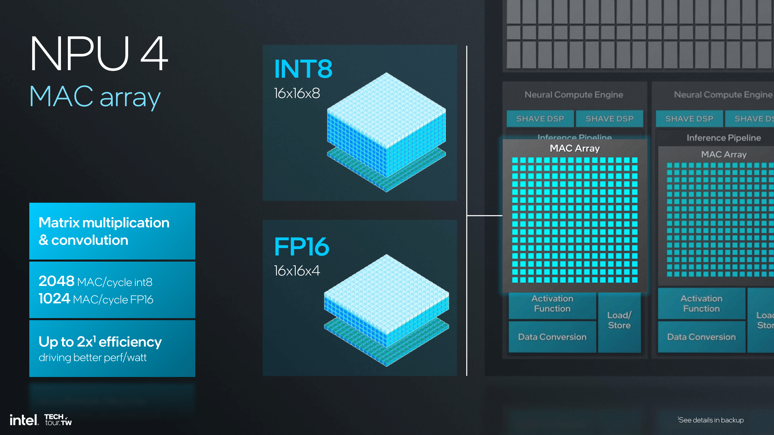
A significant improvement of NPU 4 is an increase in clock speed and introducing a new node that doubles the performance at the same power level as NPU 3. This results in peak performance quadrupling, making NPU 4 a powerhouse for demanding AI applications. The new MAC array features advanced data conversion capabilities on a chip, which allow for a datatype conversion on the fly, fused operations, and layout of the output data to make the data flow optimal with minimal latency.
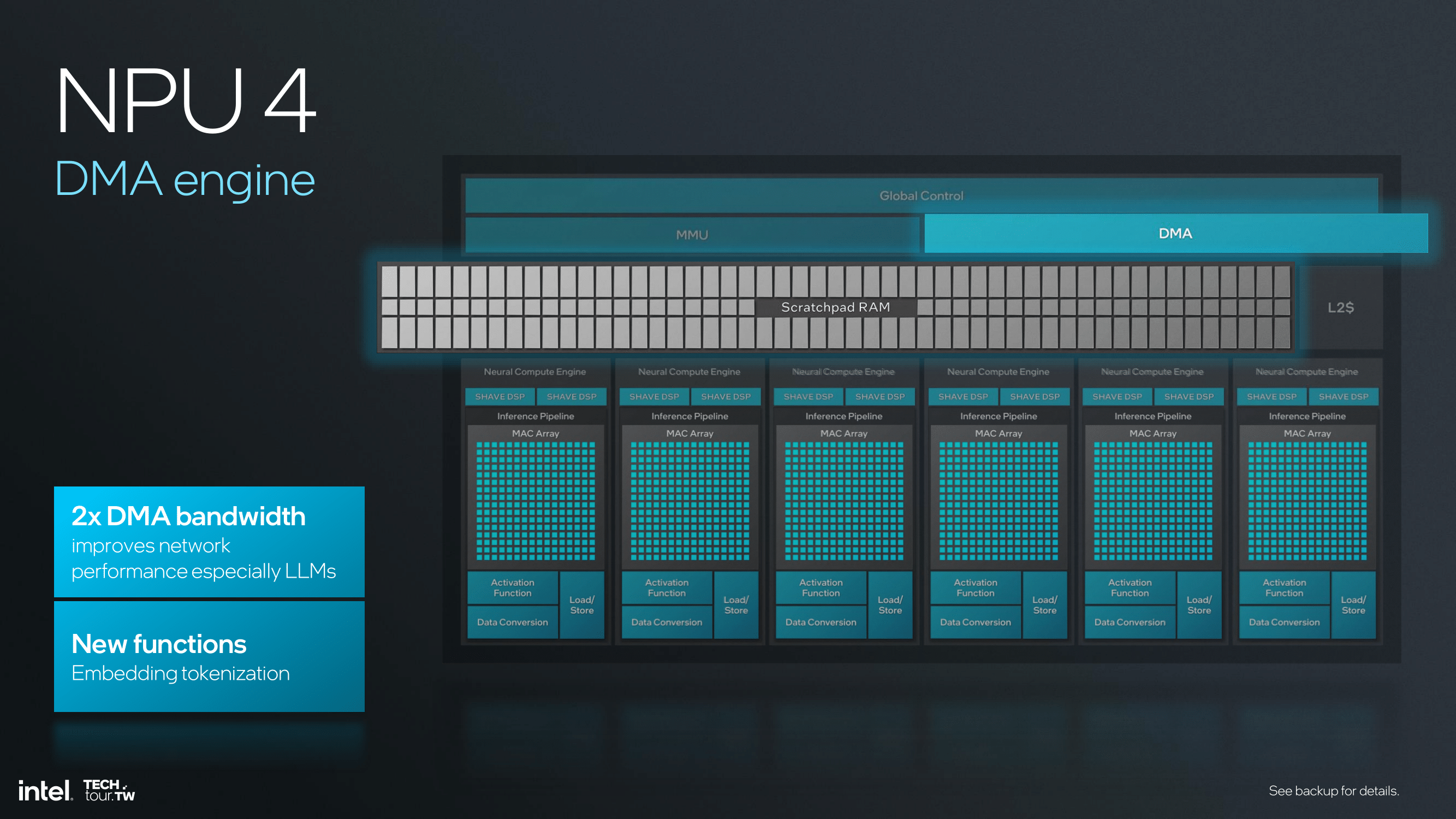
The bandwidth improvements in NPU 4 are essential to handle bigger models and data sets, especially in transformer language model-based applications. The architecture supports higher data flow, thus reducing the bottleneck and ensuring it runs smoothly even when in operation. The DMA (Direct Memory Access) engine of NPU 4 doubles the DMA bandwidth—an essential addition in improving network performance and an effective handler of heavy neural network models. More functions, including embedding tokenization, are further supported, expanding the potential of what NPU 4 can do.
The significant improvement of NPU 4 is in the matrix multiplication and convolutional operations, whereby the MAC array can process up to 2048 MAC operations in a single cycle for INT8 and 1024 for FP16. This, in turn, makes an NPU capable of processing much more complex neural network calculations at a higher speed and lower power. That makes a difference in the dimension of the vector register file; NPU 4 is 512-bit wide. This implies that in one clock cycle, more vector operations can be done; this, in turn, carries on the efficiency of the calculations.
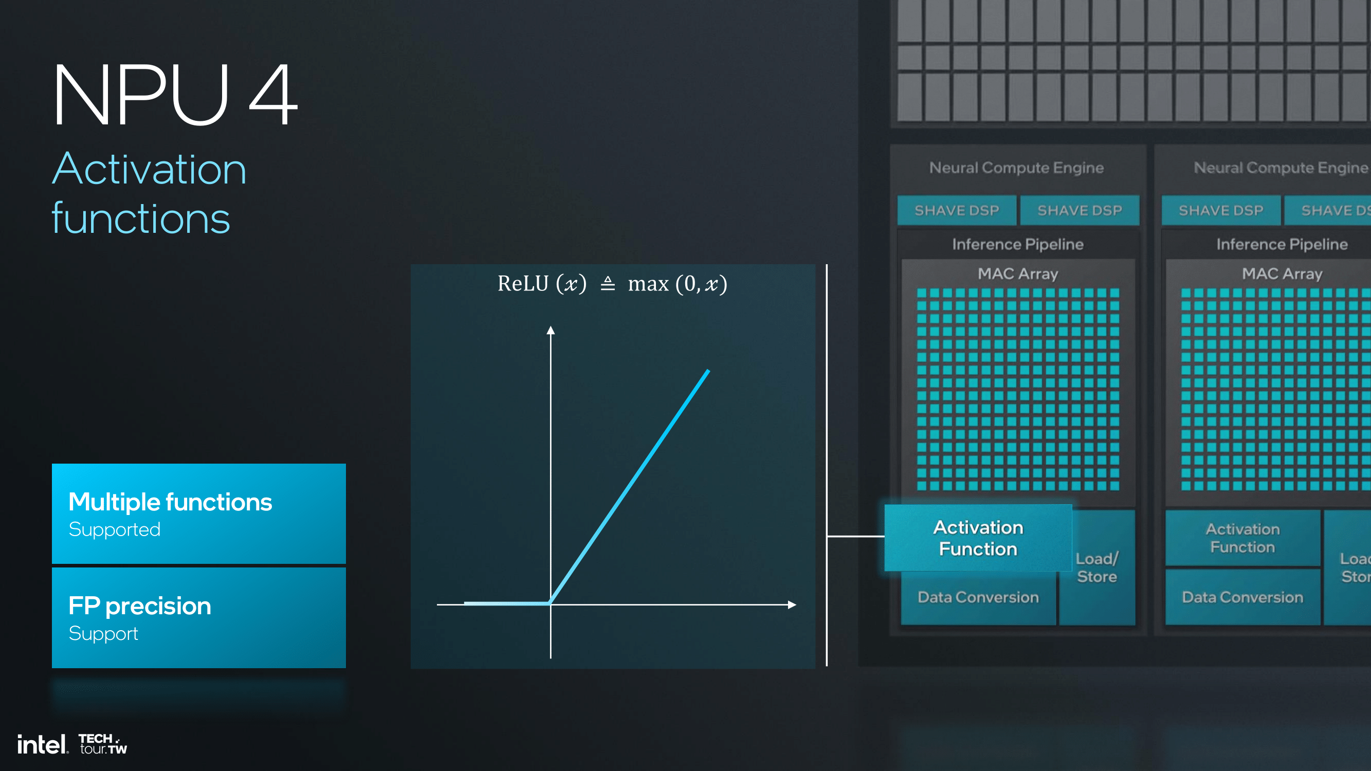
NPU 4 supports activation functions and a wider variety is available now that supports and treats any neural network, with the choice of precision to support the floating-point calculations, which should make the computations more precise and reliable. Improved activation functions and an optimized pipeline for inference will empower it to do more complicated and nuanced neuro-network models with much better speed and accuracy.
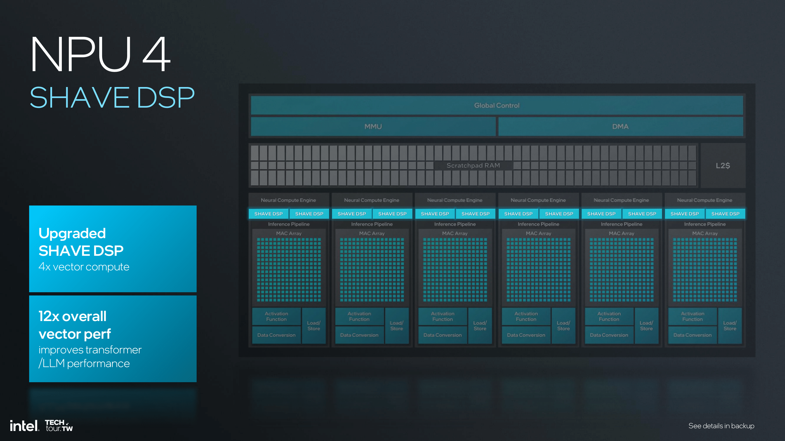
Upgrading to SHAVE DSP within NPU 4, with four times the vector compute power compared to NPU 3, will bring a 12x overall increase in vector performance. This would be most useful for transformer and large language model (LLM) performance, making it more prompt and energy efficient. Increasing vector operations per clock cycle enables the larger vector register file size, which significantly boosts the computation capabilities of NPU 4.
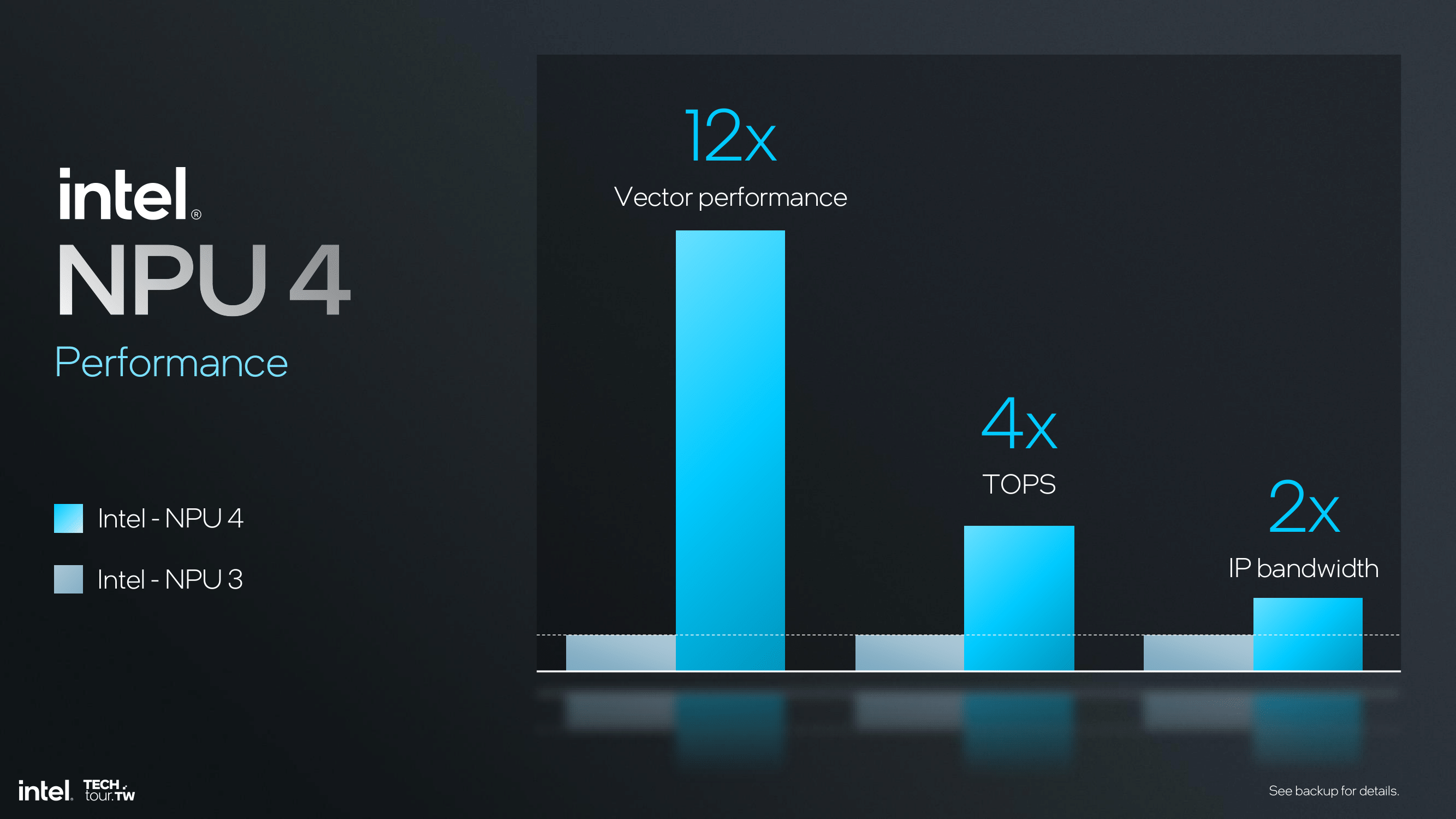
In general, NPU 4 presents a big performance jump over NPU 3, with 12 times vector performance, four times TOPS, and two times IP bandwidth. These improvements make NPU 4 a high-performing and efficient fit for up-to-date AI and machine learning applications where performance and latency are critical. These architectural improvements, along with steps in data conversion and bandwidth improvements, make NPU 4 the top-of-the-line solution for managing very demanding AI workloads.


91 Comments
View All Comments
kwohlt - Tuesday, June 4, 2024 - link
20A is best thought of as an internal only, early sampling of 18A for use on the Compute Tile.But LNL differs from ARL in that its compute tile also contains the iGPU and NPU, making 20A not an appropriate choice. 18A would've been the node Intel would've needed, but that's not until next year (coincidently, LNL's direct successor, PNL, will use 18A for it's unified compute tile instead of TSMC) Reply
Blastdoor - Wednesday, June 5, 2024 - link
Or we could take it to mean that intel reserved a lot of N3B capacity and so figured they might as well use it. Like Apple, they will probably be looking to get off of N3B ASAP. While Apple moves to N3E, Intel will leap ahead to A18. ReplyThe Hardcard - Wednesday, June 5, 2024 - link
Barring newly announced delays, TSMC will hit volume on N2 in the same timeframe as volume on Intel A18. Apple’s move to N3E has happened. N2 in 2025. Replyrgreen1983 - Tuesday, June 4, 2024 - link
"This uplift is noticed, especially in the betterment of its hyper-threading, whereby improved IPC by 30%, dynamic power efficiency improved by 20%, and previous technologies, in balancing, without increasing the core area, in a commitment of Intel to better performance, within existing physical constraints."So hyper threading is bother present and improved, yet they disabled it? This seems non sensical Reply
meacupla - Tuesday, June 4, 2024 - link
From what I have read and seen from other tech sites, Intel disabled HT because it wasn't working properly with E-cores.Disabling HT improves performance and efficiency, because the E-cores get utilized, instead of sitting idle on low power loads. Reply
rgreen1983 - Tuesday, June 4, 2024 - link
I'm not asking why they disabled HT, we've known they were going to disable HT for some time. Disabling HT out of the box doesn't do anything because we've always been able to disable HT ourselves. I'm asking why they improved it if they are going to disable it, why waste a bunch of transistors and die area on a disabled feature? And if maybe the decision came too late to be removed, why brag about a thing that isn't even enabled? ReplyDrumsticks - Tuesday, June 4, 2024 - link
Unfortunately, this feels like word salad from Anandtech. I won’t speculate how or why it was left in, or why Anandtech is quoting a 30% gain in IPC that is nowhere in Intel’s slides or on other tech website coverage.They didn’t improve hyperthreading and then disable it. They removed the feature completely, and netted the die area and power savings from doing so. They probably also took a MT loss, but the die area and power savings could have been redirected to either better usage of the area for more performance, or just direct cost and efficiency savings. Intel’s hyperthreading was always a really inefficient way to gain a small amount of performance anyways. The actual side, published on Techpowerup’s dive, says removing hyperthreading saved them 5% perf/power, 15% perf/area, and 15% perf/power/area. That slide doesn’t appear to be published on Anandtech.
Essentially, they didn’t waste a bunch of transistors on a disabled feature - they did the obvious thing and physically removed the feature from the die. The description here is Anandtech’s fault, not Intel’s. Reply
rgreen1983 - Tuesday, June 4, 2024 - link
Thank you for your reply and the suggestion to check the techpowerup article. I would expect you are correct like the techpowerup article that HT was removed from the design and silicon, but I've also just read the pcworld lunar lake article which seems to suggest otherwise and amazingly has a slide not found in the techpowerup or anandtech articles.What I think might be going on is that lion cove still has HT in the design because Intel wants it for server chips, although I'd argue it's not necessary there either and by the looks of their recent all E core xeons the thread count sensitive clients should be running those anyways. That would explain why they might improve HT. If that is the case is there 2 lion cove designs, one with HT and another without? I just read the wccftech article which suggests this is the case, mentioning "variants" of lion cove.
Since this lion cove core for lunar lake is being made at tsmc, it makes sense they had to make a new design for their fab anyways so maybe they did remove HT, and wccftech says they removed TSX and AMX also. So the lion cove for Intel fab coming to arrow lake/xeon might have HT, will definitely have TSX and AMX, but they might still turn HT off and only enable for xeon.
Regardless yeah the anandtech mention of HT improvements here in relation to lunar lake seems off base. But I still think there is more Intel could clear up on HT status on die and whether there are multiple lion cove designs. Reply
Drumsticks - Tuesday, June 4, 2024 - link
I think they (techpowerup and pcworld) are both right. Per Tomshardware, commenting on Intel removing HT:"As such, Intel architected two versions of the Lion Cove core, one with and one without hyperthreading, so that the threaded Lion Cove core can be used in other applications, like we see in the forthcoming Xeon 6 processors."
I expect the LNL physical design lacks HT, as that's the only way to actually get the performance/area and performance/watt savings. But we'll probably see the version of Lion Cove with hyper threading show up in the Xeon world (although, to be honest, I'm not sure if it's worth it there given the efficiency losses), as well as on Arrow Lake, where higher performance in exchange for an efficiency loss tends to be an acceptable tradeoff for PC Enthusiasts.
The Tomshardware article also points out to me where Anandtech's article summary gets the 30% number: "Intel’s architects concluded that hyperthreading, which boosts IPC by ~30% in heavily threaded workloads, isn’t as relevant in a hybrid design that leverages the more power- and area-efficient E-cores for threaded workloads." - this is coupled with yet another slide that shows Intel quoting hyperthreading as a +30% throughput for +20% Cdyn.
In other words, I think *lunar lake* does not feature hyperthreading - it's physically non-present in the design. Lion Cove the P-Core microarchitecture, on the other hand, has two designs - one with HT physically present (in Arrow Lake and any Xeon SKUs - speculation), and one without (in Lunar Lake only).
On that note, it also implies two different Modules for e-core as well - one with the e-cores not present on the ring bus (in Lunar Lake) and one where it's connected to the ring bus like "normal"
- this being the config in Alder Lake and Raptor Lake (and this is presumably coming in Arrow Lake higher power laptop SKUs and the desktop) Reply
rgreen1983 - Wednesday, June 5, 2024 - link
Thank you for indulging me in this detailed discussion. I think you are right there are 2 lion cove designs. I don't think all the news outlets are aware of it. Reply